EXPERIMENT 1: SWITCHING CHARACTERISTICS OF POWER DIODES
1. Objective.
The objective of this experiment is to demonstrate the dynamic and switching characteristics of power diodes.2. Background.
The switching characteristics of the diode are determined by the capacitive properties of the pn-junction. Studying these dynamics helps to understand the more complex switching behavior of other semiconductor devices. There are two distinct switching transients.2.1. Turn on Transients.
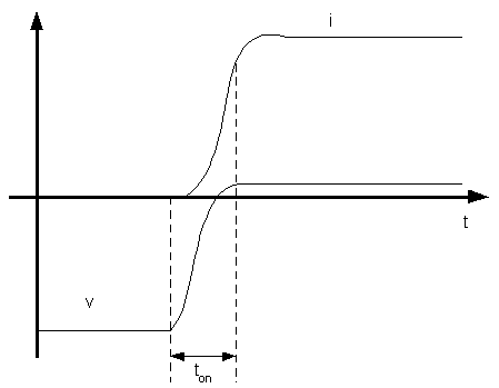
With reference to Figure 1.1, the diode turn-on is delayed by the junction capacitance. Thus, if foreword voltage is applied across the diode, a small charge of minority carriers is stored in the junction and the diode commences conduction.With reference to Figure 1.1, the turn-on time can be measured from the beginning of the rising of the anode current to the moment this current reaches 90% of its forward conduction value.
Fig. 1.1. Current and voltage during diode turn-on.
2.2. Turn-off Transients.
When the diode has been conducting, a significant charge is stored at the junction and the bulk of the semiconductor. With reference to Figure 1.2, when the diode current becomes negative, the diode continues to conduct. This reverse conduction continues until the negative current sweeps away the minority carriers stored in the junction. At that moment, the diode gains its reverse blocking capability and its voltage charges to the reverse recovery voltage. The time needed for the diode to gain blocking capability is denoted by ta. An additional time, tb, is needed to remove the minority carriers from the bulk of the semiconductor. Therefore, the total turn-off time is the reverse recovery time of the diode, trr=ta+tb. The total charge that must be removed during reverse recovery is denoted by QRR i.e. the reverse recovery charge. This charge is given as a diode parameter. The peak negative current during reverse recovery is denoted by IRR. Figure 1.2 provides the relations applied to the diode turn-off.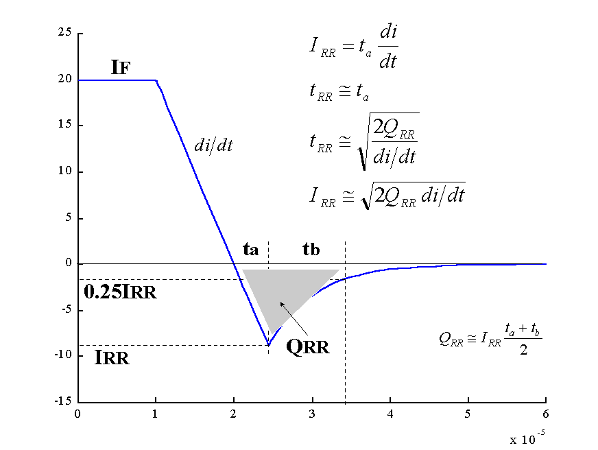
Fig. 1.2. Current during diode turn-off.
The total switching time of the diode is tsw=ton+trr. The switching time of the diode limits the switching frequency of the supply.
Abrupt turn-off may occur as a result of un-damped oscillations. These oscillations arise due to resonance formed between the junction capacitance and the circuit inductance. The overvoltage in abrupt recovery can damage the diode. A commonly used protection is the snubber shown in Figure 1.3. A simple snubber consists of a capacitor and a resistor in series. The resistor introduces damping and the capacitor decreases the oscillation frequency.
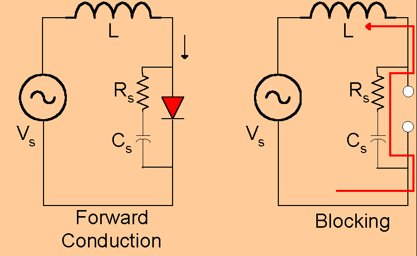
Fig. 1.3. Application of the snubber in diode turn-off.
3. Equipment.
HP-VEE set-up
1N5404G18451 Power diode
1N5242B Fast switching diode
2W and 50W Single resistors
2kW Potentiometer
1mF Capacitor
Inductor box (1, 4.7, 10, 1000 mH)
4. Procedure.
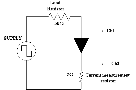
Fig. 1.4. Experimental set-up for obtaining diode dynamic response.
5. Report.