EXPERIMENT 3: THYRISTOR RECTIFIERS
1. Objective.
The objective of this experiment is to study the control and operation of the single-phase full thyristor-bridge. The control and gate drive circuit of the bridge is examined. The waveforms of the bridge are studied under resistive load and under continuous conduction. The inverter operation is also demonstrated. The steady state relation between the dc quantities and the control quantities of the bridge is verified experimentally.
2. Background
The output of thyristor rectifiers provides a dc voltage with variable average value. The average voltage can be controlled and adjusted electronically by delaying the current pulse to the thyristor gates. Full wave rectifiers are constructed based on the topology of the full-wave bridge. The bridge can operate as a rectifier or as an inverter.
2.1. Rectifier Operation.
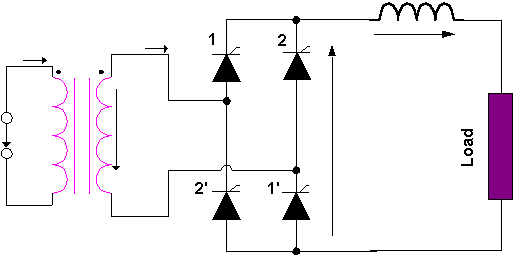
Figure 3.1 depicts a full-bridge thyristor rectifier. Its topology is similar to the full-bridge diode rectifier. The smoothing reactor in series with the load reduces the ripple of the dc current and extends the range of the continuous conduction.
Fig. 3.1. The topology of a full-bridge thyristor rectifier.
With reference to Figure 3.2, Thyristors 1 and 1' are ignited in the positive semi-period of the line voltage and at a moment delayed from the positive zero-cross by the amount of the ignition delay angle, a. With reference to Figure 3.2, if the conduction of the dc current is continuous, Thyristors 1 and 1' will conduct until the ignition of the pair 2 and 2'. In symmetric operation of the bridge, Pair 2-2' is ignited in the negative semi-period of the line voltage and with the same delay from the negative zero-cross as the pair 1-1'. Equation 3.1 provides the value of the average dc voltage for continuous conduction.
![]() (3.1)
(3.1)
Where, Vs is the rms value of the line voltage.
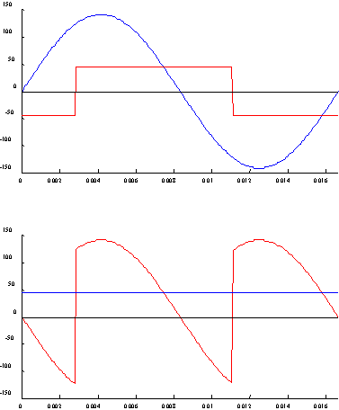
Fig. 3.2. Rectifier output.
Figure 3.2 shows the waveforms of the dc voltage and ac current obtained from the rectifier under continuous conduction and for large value of the smoothing reactance. As it is seen from the figure, the ac current of the rectifier is a square pulse, whose fundamental component is given by (3.2). The fundamental of the rectifier current lags the line voltage by the ignition delay angle. Thus from the ac side the bridge, when operating as a rectifier, is seen as an inductive load.
![]() (3.2)
(3.2)
Where, Id is the average value of the dc current.
2.2. Inverter operation.
Inverter operation commences when the ignition delay exceeds 90° . According to (3.1) for continuous conduction, the average dc voltage becomes negative. Thus, it is necessary that the dc load have a source to maintain the flow of current. The inverter circuit is drawn as in Figure 3.3, where the numbering (and ignition sequence) of thyristors is identical with that in Figure 3.1.With reference to Figure 3.3, the dc source supplies the power. The dc terminals of the inverter act as a load to that source. Figure 3.4 shows the waveform of the dc voltage for the inverter of Figure 3.3. The waveform of the ac current is shown in the same figure. With reference to Figure 3.4, the ac current of the inverter lags the line voltage with a negative power factor. Therefore, the inverter injects power into the ac system. Its ac terminals appear as an inductive source.
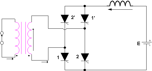
Fig. 3.3. The topology of the single-phase inverter.
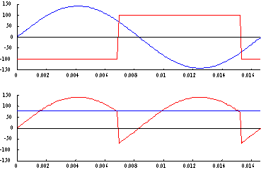
Fig. 3.4. Inverter output.
2.3. Control and Firing of Thyristors.
The Thyristor Bridge is a line-commutated converter. Therefore the firing pulses to the thyristors must be delivered synchronously with the line voltage. An additional external circuit is needed to generate the firing pulses. The objective of a control and firing circuit is to synchronize the firing pulses to the zero-cross of the line voltage, to delay the firing pulses by a controllable delay, and to amplify and supply these firing pulses to the gate of the thyristors.A typical arrangement of a control and firing circuit is shown in Figure 3.5. The first stage is a control transformer for stepping down the line voltage to a level suitable for the control circuit. The secondary of the transformer is fed to the zero-cross detector. This stage typically marks the moments of the transition between positive and negative values of the line voltage by short pulses. These pulses denote the moment of the zero-cross and synchronizing the control circuit with the frequency of the line.
In systems, where the ac supply has high impedance, the non-sinusoidal current of the bridge causes distortion of the line voltage. The result of the distortion of the line voltage waveform is multiple zero crossings and zero-cross jitter. The latter means that the zero-cross frequency fluctuates. The former means that more than one zero crossing may occur around the zero-cross of the fundamental of the line voltage. Multiple zero-cross and zero-cross jitter could result in unsymmetrical firing of the bridge. This in turn can re-enforce the distortion of the line voltage. This positive feedback loop in some cases result in what is known as harmonic instability.
In order to prevent unsymmetrical operation, the zero-cross detector is equipped with hysterisis comparators and a phase locked loop (PLL). The former eliminates multiple zero crossings. The latter stabilizes and locks the frequency of the detection pulses to the line fundamental zero-crossings.
The next stage of the control and firing circuit is the firing pulse generator. This stage typically utilizes the zero-cross pulses of the previous stage to generate a periodic ramp of twice the frequency of the fundamental. The ramp is reset and commences rising with the onset of each zero-cross pulse. This ramp is compared with a reference voltage provided externally. The level of this voltage is proportional to the desired ignition delay angle. A short firing pulse is generated at the moment the ramp exceeds the reference voltage. Thus, if the reference voltage is near zero, the firing pulse will be generated near the line zero-cross. This corresponds to low value of a. As the level of the reference voltage increases, the firing pulse is delayed away from the line zero-crossings.
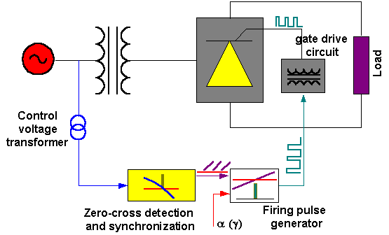
Fig. 3.5. Block diagram of the control and firing circuit.
The final stage is the gate drive circuit. This stage amplifies, shapes and delivers the firing pulses to the gate of the thyristors. In the majority of applications galvanic isolation is needed between the drive circuit and the thyristor gate. This isolation may be provided through pulse transformers, opto-couplers, or optical fiber cable (for light triggered thyristors, LTSCR).
2.4. The EMIL2000-LX Gate Drive and Control System.
The EMIL2000-LX is an implementation of a control and firing circuit based on analogue and integrated electronics. The schematic of the EMIL2000-LX is shown in Figure 3.6. The circuit has three stages.
Fig. 3.6. Schematic representation of the EMIL2000-LX control and gate drive circuit.
With reference to Figure 3.6, the input to the zero-cross detector is the line voltage from the control transformer. The zero-cross detector is a window comparator employing two op-amps. Figure 3.6 explains the operation of the comparator. In the lower comparator, the negative line voltage is compared with the zero level. Thus, this comparator is high, when the line voltage is negative and low, when the line voltage is positive. The upper comparator compares the positive line voltage with the level of 0.7V. Thus, the output of this comparator is high when the line voltage exceeds 0.7V and low otherwise. The output of both comparators is "ORed" through two diodes. The combined output is a negative notch at the arrival of a zero crossing. Figure 3.6 depicts these waveforms in relation to the line voltage. The negative notch is inverted through a transistor and a short pulse is obtained at the output of the stage, which is synchronous to the line zero-cross. Figure 3.7a shows the line voltage and the output of the zero-cross detector.
The next stage of the EMIL2000-LX is the phase control circuit. With reference to Figure 3.6, a -6V supply is connected to the input of an integrator, through a potentiometer. The output of the zero-cross detector activates a MOS-FET switch that is connected across the terminals of the integrator capacitor. The capacitor voltage increases linearly as it integrates the constant input to the integrator. At the arrival of the zero-cross pulse, the MOS-FET is activated and the capacitor terminals are shorted. This causes the capacitor to discharge through the MOS-FET resistance. The voltage of the capacitor is decreased to almost zero. At the end of the zero-cross pulse, the MOS-FET is deactivated and the capacitor commences charging again. This produces the periodic ramp of Figure 3.7b.

Fig. 3.7. Firing waveforms of the EMIL2000-LX. (a) Commutating voltage and zero-cross detection, (b) synchronous ramp and ignition-delay reference.
With reference to Figures 3.6 and 3.7b, the integrator ramp is compared with a variable reference voltage to produce the firing pulses. These pulses are amplified before delivered to the gate drive circuit. With reference to Figure 3.6, the gate drive circuit consists of four pulse transformers delivering the firing pulse between the gate and cathode of the bridge thryristors. A transistor drives the transformers. When the firing pulse arrives, the transistor saturates essentially connecting the primary of the transformer to the +6V supply. The diode across the primary is needed to circulate the magnetizing current of the transformer, when the pulse is removed and the transformer is essentially disconnected from the supply. All pulse transformers are driven simultaneously by the firing circuit. Thus, the four thyristors receive firing pulses simultaneously, however, only the thyristors with forward voltage with ignite.
3. Equipment.
HPVEE setup
LEADER LBO-516 Oscilloscope
H-R-SCR tri-voltage power supply
H-R-SCR-2A thyristor module
H-R-SCR-2C Loads
LabVolt EMS 8321 (variable [switched] inductance)
ACME 13X Control transformers
EMIL2000-LX Gate-drive and control system
HMD-100 PPC-DC 0-125V variable dc power supply.
4. Procedure
5. Report